SEMICON Taiwan 2025: The Era of Heterogeneous Integration Arrives - Materials Become the New Core of Semiconductors
As AI, HPC, 5G, and autonomous driving applications continue to accelerate, chip design has evolved from single die wafer logic to the era of System-in-Package (SiP) and heterogeneous integration.
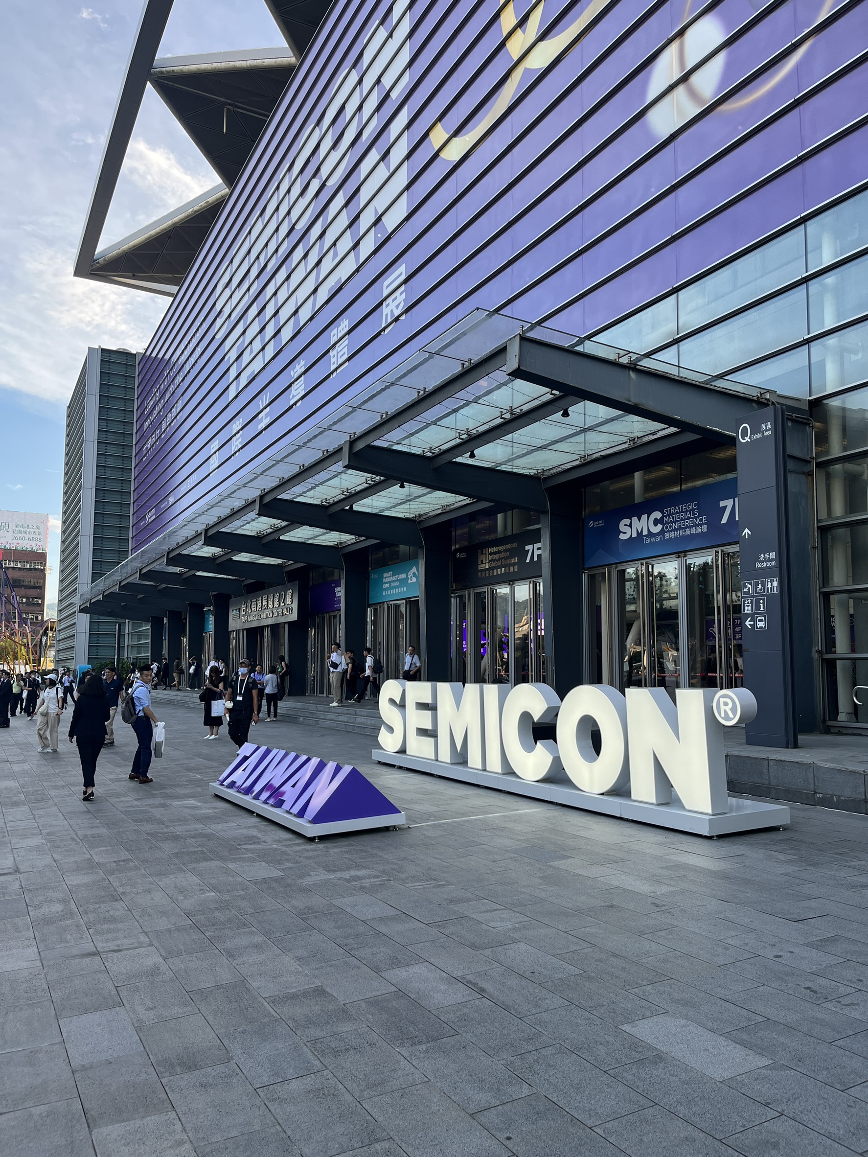
At SEMICON Taiwan 2025, Silicon Photonics and 3D-IC stacking once again take center stage. Most exhibitors are presenting solutions around these two themes—reflecting not only architectural innovation but also a new “materials battlefield.”Today, key parameters such as dielectric constant (Dk), dielectric loss (Df), coefficient of thermal expansion (CTE), optical refractive index, and material reliability directly determine system performance and manufacturing yield.
For Taiwan, the competitiveness in heterogeneous integration now lies not only in equipment and foundry capability but also in high-performance materials sovereignty.
As Globalwafers Chairwoman Doris Hsu remarked:“The next bottleneck may no longer be process technology—but critical materials.”
Below are several highlights from this year's exhibition.
1. The Technological Turning Point: From Electrical to Optical Interconnect
Traditional packaging relies on electrical interconnects, but as inter-chip data transmission surpasses 100G/400G, issues such as signal loss, crosstalk, and latency have emerged.
Silicon Photonics (SiPh) has thus become the next-generation solution—replacing copper lines with optical waveguides to achieve low latency and low power consumption at high speed.
However, SiPh packaging introduces new material challenges:
- Waveguide layers require high–low refractive index contrast.
- Fiber-to-chip coupling interfaces demand optically transparent and thermally stable resins.
- Packaging materials must feature low moisture absorption, high optical transmittance, and low stress.
Here, silicone and acrylic resins play critical roles.
High-index silicones (n ≈ 1.52–1.55) serve as core layers, while low-index acrylics (n ≈ 1.40–1.43) function as cladding layers, forming stable optical pathways.
Moreover, incorporating hollow silica or fluorinated nano-fillers further lowers refractive index and dielectric constant (Dk < 2.5), supporting high-speed optical interconnects with reduced delay and power loss.

2. 3D IC and the Thermal Management Challenge
3D ICs vertically integrate logic, memory, and module components through TSV (Through-Silicon Via) and micro-bump connections.
While this dense stacking boosts computing performance, it introduces severe thermal conduction and stress management challenges.
Conventional epoxy resins, though offering strong adhesion and insulation, often suffer from thermal fatigue and dielectric degradation under high-power, high-temperature conditions.
Thus, material innovation is moving toward:
- Low CTE, high thermal conductivity, and low dielectric loss (Df);
- Filler hybridization and structural tuning.
Examples include:
Boron nitride (BN): High thermal conductivity (>40 W/m·K), electrically insulating, and low-Dk—ideal for resin or dielectric fillers.
Silicon carbide (SiC): Reinforces mechanical rigidity and suppresses thermal deformation.
Spherical silica: Reduces dielectric constant and improves dimensional stability.
Compatibility between fillers (BN, SiC, SiO₂) and resin matrices (epoxy, silicone, acrylic) depends on surface treatment and dispersion technology.
Optimized dispersants and leveling agents ensure uniform nano-filler distribution, minimizing voids, stress accumulation, and reliability failures.
3. Low-Dielectric Materials: The Key to High-Speed Signal Integrity
For both SiPh modules and 3D IC dielectric layers, low dielectric constant (Low Dk) and low loss (Low Df) have become essential.
Even a 0.1 reduction in Dk can lead to significant improvements in signal delay and power efficiency.
Current material R&D focuses on:
- Hollow silica spheres or organically modified SiO₂: Maintain mechanical strength while lowering Dk and Df.
- Fluorinated resins or acrylics: Replace C–H bonds with C–F to minimize polarization loss.
- Hybrid resin systems: Combine epoxy's mechanical strength with silicone's low-Dk performance, achieving balanced Dk < 2.8.
These materials extend beyond dielectric layers to Co-Packaged Optics (CPO) and SiPh modules—serving as underfills, adhesives, and optical claddings.
4. Material Sovereignty: From Supply Chain Risk to Strategic Asset
Another major theme at SEMICON 2025 is Material Sovereignty.
In the AI and advanced packaging era, foundries and OSATs alike now realize that material control = national competitiveness.
Historically, high-performance resins, fillers, and additives were heavily dependent on overseas suppliers.
However, global tensions and export restrictions have driven Taiwanese companies to accelerate local material formulation and integration capabilities.
At Globe Union Group, we have long specialized in electronic materials, partnering with global leaders across the U.S., Europe, Japan, and Korea to offer:
- Epoxy, silicone, acrylic, and specialty resins—for optical clarity, low stress, thermal resistance, and high electrical performance.
- Functional fillers—TiO₂, SiO₂, BN, SiC, hollow silica, Al₂O₃—for tailored thermal, dielectric, and refractive needs.
- Additives—dispersants, leveling, and defoaming agents—to optimize formulation stability and processing reliability.
Through cross-material integration, we deliver not only products but complete materials-engineering solutions, ensuring process consistency from pilot to mass production while securing stable supply partnerships.
5. Conclusion: Materials Innovation Driving the Future of Heterogeneous Integration
SEMICON Taiwan 2025 showcases more than tools and processes—it reflects a materials awakening across the semiconductor ecosystem.
From chip design and packaging to optoelectronic integration and system-level cooling, every leap in performance is powered by breakthroughs in materials science.
As Silicon Photonics and 3D IC technologies approach mass production, the materials supply chain faces a critical upgrade.
The ability to deliver low-Dk × high-thermal × high-reliability × optically stable materials will be the foundation of true heterogeneous integration.
Looking forward, we will continue collaborating with customers and R&D partners to develop more competitive formulations through our Resin + Filler + Additive integration model—helping Taiwan advance from a manufacturing powerhouse to a materials powerhouse on the global semiconductor stage.

#SEMICON Taiwan #NegativeCTE #NTE #WarpageControl #LowDk #LowDf #SiliconPhotonics #HeterogeneousIntegration #3DICStacking #MaterialSovereignty #LowRefractive #HighRefractive
CONTACT US
Kelly Chemical Corporation
Electronics
TEL:(02)2762-1985 ext 11200
Online Message
Leave your contact information,
and we will get in touch with you soon.
Email Consultation
After receiving your email,
we will process it as soon as possible.send Email


