The Glue Alliance: the super heros in semiconductor
Behind every chip, from the critical materials used in production to the final packaging that protects and keeps it running, it’s hard to imagine just how many materials quietly hold everything together.
While you use your phone or computer in your everyday life, you probably never think about the chips powering these devices are as fragile as thin glass.
During manufacturing, these chips fear scratches, shocks, and heat—one misstep and they could be scrapped. So how do they survive this series of harsh trials to finally make their way into our devices?
There's a class of materials you won't see in news headlines or on your phone's spec sheet—yet they're the unsung heroes ensuring every chip travel safely from the factory to your hands.
They are the "Glue Alliance"
—the superheroes of the semiconductor world!
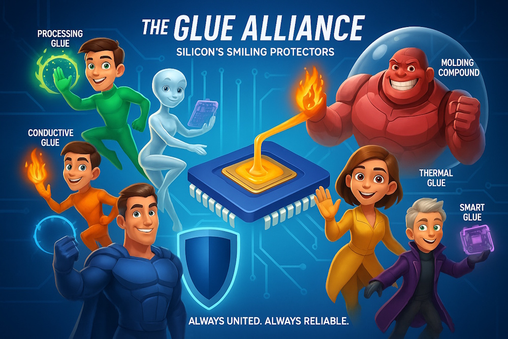
These glues act like invisible umbrellas, taking care of chips every step of the way—from their creation to going live in devices.
If semiconductor manufacturing were an adventure, the chip would be the protagonist, and this group of specialized glues would be the heroes guarding it along the journey.
Some serve as protectors, shielding the wafers from scratches and contamination during processing; some are architects, firmly anchoring the chip onto its substrate; others are thermal experts, ensuring the chip doesn’t overheat and crash.
Each glue has its own unique ability, and no single one could do it alone. But together, they ensure the chip safely completes its evolution, becoming the core that powers modern life.
The "Glue Alliance" : Different Glue, Different Role
1. The Protector: Temporary Protective Coatings
In semiconductor manufacturing, a wafer is like a thin sheet of glass. Any scratch, contamination, or even slight chemical erosion can ruin the entire wafer. To help it survive the harsh steps of etching, grinding, and cleaning, engineers apply a temporary protective coating. This coating isn't meant to stay forever—it's a short-term guardian, much like how a patient wears a sterile surgical gown before an operation.
However, applying this protective glue is not as simple as slapping it on. If the chip were a smartphone screen, the protective coating would be like a screen protector: you need a scratch-resistant type, it must be applied smoothly, and when it's time to replace it, it should come off cleanly without damaging the screen. In semiconductors, the environment is even more demanding. The coating must withstand high temperatures, high pressures, and strong acids or bases, all while not interfering with subsequent processes.
These protective glues appear in different forms depending on their use case. Common types include the following:
- Wafer Thinning (Back Grinding)
During the process, wafers must be ground from several hundred micrometers thick down to just a few tens of micrometers to meet packaging requirements. However, the thinner the wafer, the more fragile it becomes—just like glass. At this stage, the protective coating is applied to the front side of the wafer to support its structure and absorb stress, ensuring it does not break from vibration or pressure during back grinding.
- Etching and Wet Processes (Etching / Cleaning)
During chemical etching or cleaning, wafers are exposed to strong acids, bases, or other corrosive chemicals. Without a protective coating, the circuitry areas could be damaged, resulting in wafer rejection. Temporary protective coatings act like a transparent shield, isolating sensitive areas from chemical contact. Once the process is complete, the coating is removed, allowing the chip to safely proceed to the next stage.
- Temporary Bonding
With advances in wafer thinning, traditional vacuum suction or mechanical clamping methods can no longer meet the requirements. Temporary bonding technology emerged as a solution. The wafer is fixed onto a stable support substrate, essentially giving it a "backboard" that provides mechanical strength and stability, facilitating subsequent thinning or dicing processes.
- Wafer/Die Protection and Handling
Throughout the semiconductor supply chain, wafers or dies undergo multiple transfers, dicing, and testing steps. Even tiny scratches or particles can cause chip failure. Using protective coatings to prevent physical damage is like giving the chip an invisible armor, playing a critical role in maintaining high product yields.
These varying application scenarios also determine that temporary protective coatings must be designed with diverse formulations and material choices. They need to withstand mechanical grinding pressures, resist chemical corrosion, and remain stable under high temperatures—yet still be easily and cleanly removed.
The table below summarizes common application scenarios, required properties, and possible resins or materials, providing a clear view of the multifaceted roles these coatings play in semiconductor manufacturing.
| Application Scenario | Material Property Requirements | Common Materials |
|---|---|---|
| Wafer Thinning (Back Grinding) | High toughness, pressure-resistant, able to absorb mechanical stress; can be cleanly removed after grinding without leaving residues | Thermoplastic elastomers (TPE), Polyurethane (PU), Acrylic resins, Some silicones |
| Etching / Wet Processes (Etching / Cleaning) | Resistant to acids and bases, solvent-resistant, chemically inert; must be fully removable in subsequent steps | Polyimide (PI, peelable type), Acrylic, Fluoropolymers (e.g., PTFE derivatives), Some hydrolyzable polymers |
| Temporary Bonding | High adhesion, withstands high-temperature processes; must be reversibly removable later (UV, thermal decomposition, dissolution) | UV-release acrylics, Thermally-decomposable epoxy/phenolic, Siloxane-based systems |
| Handling / Storage (Pre-Packaging) | Scratch- and dust-resistant, moderate adhesion; must be easy to peel off | Peelable acrylics, Polyvinyl alcohol (PVA, water-soluble), Peelable silicone films |
2. The Connector: Die Attach Adhesives
Once a chip is diced from the wafer, it needs to be securely mounted on a substrate before subsequent electrical connections and packaging steps can take place.
This is where Die Attach adhesives come into play.
Its role is much like a building architect laying a foundation—it firmly anchors the chip in place, allowing it to withstand thermal processes and long-term operational conditions. Without this layer, the chip could loosen due to thermal expansion, contraction, or moisture ingress, potentially causing the entire electronic system to fail.
Although all involve bonding the chip to another surface, Die Attach adhesives must be specifically designed to meet the demands of different application scenarios. Some common use cases include:
- Standard Die Bonding
In traditional packaging, the chip must be fixed onto a metal or organic substrate. Die Attach adhesives provide adhesion and interfacial stability, ensuring the chip does not shift before electrical connections are made.
- High-Power Devices
Power chips such as IGBTs, MOSFETs, or SiC/GaN devices generate significant heat during operation. In this case, Die Attach adhesives must not only secure the chip but also provide high thermal conductivity to efficiently transfer heat away.
- Optoelectronics and LED Packaging
Unlike standard logic ICs or power devices, applications like LEDs and optical sensors require Die Attach adhesives to combine thermal conductivity with optical stability, preventing performance degradation under prolonged exposure or high temperatures. Die Attach adhesives for optoelectronics and LEDs often incorporate high thermal conductivity fillers such as silver, aluminum oxide, or aluminum nitride to rapidly dissipate heat.
- Advanced Packaging (Flip Chip, 2.5D/3D ICs)
As chips become thinner and I/O counts increase, Die Attach adhesives must feature low coefficient of thermal expansion (CTE) and compatible flow characteristics to work in harmony with subsequent materials such as underfills or moldable underfills (MUF).
Unlike temporary protective coatings, Die Attach adhesives serve as the chip's long-term anchor. They must firmly fix the chip to the substrate while also providing thermal and electrical conductivity, optical stability, and compatibility with subsequent underfill or molding compounds. Depending on the application, Die Attach formulations can vary significantly to meet these specific requirements.
| Application Scenario | Material Property Requirements | Common Materials |
|---|---|---|
| Standard Die Bonding | High adhesion, good interfacial stability; must withstand post-process electrical testing and packaging stresses | Epoxy resins, modified epoxies, epoxy with small amounts of fillers |
| High-Power Devices | High thermal conductivity, high-temperature resistance; prevents chip overheating and failure | Silver-filled epoxy, thermally conductive epoxy with fillers (AlN, BN) |
| Optoelectronics and LED Packaging | Combines thermal conductivity with optical stability; prevents yellowing or performance degradation from prolonged exposure | Silver-filled epoxy, thermally conductive epoxy (aluminum oxide, aluminum nitride), silicone-based adhesives |
| Advanced Packaging (Flip Chip, 2.5D/3D ICs) | Low coefficient of thermal expansion (low CTE), compatible flow properties; must work in conjunction with underfill/MUF | Low-CTE modified epoxies, hybrid resins (co-designed with underfill) |
3. The Reinforcers: Underfill, MUF, and Molding Compounds
Once the foundation is firmly in place, the next step is the “casting” process.
The core function of these materials is to address stress issues caused by differences in thermal expansion (CTE) between the chip and the substrate.
Different materials have different coefficients of thermal expansion (CTE). During repeated temperature cycles from turning devices on and off, the chip and substrate act like two metal sheets expanding and contracting at different rates. This can pull and deform solder joints, potentially causing cracks and eventual failure.
Underfill, MUF, and molding compounds fill, reinforce, and distribute these stresses—making this a critical aspect of semiconductor packaging.
The specific materials and casting processes vary depending on the application scenario. Some common use cases include:
- Flip Chip Packaging Underfill
In Flip Chip structures, the chip is mounted upside down and connected directly to the substrate via solder bumps, which are extremely fragile. The solder joints between the chip and substrate are as fine as a hair. Without underfill reinforcement, it’s like a bridge without steel reinforcement—the joints can quickly crack due to thermal expansion and contraction. The underfill adhesive fills the gaps between the solder bumps, transferring stress from the delicate joints to the entire interface, significantly improving reliability.
- Fan-Out / WLCSP – MUF
MUF acts like an all-in-one casting process, eliminating the traditional two-step sequence of gap filling followed by molding. This approach is particularly suitable for advanced packaging where chips are thinner and I/O counts are higher. By combining underfill and molding into a single step, MUF not only improves process efficiency but also better meets the demands of increasingly thin and highly integrated designs.
- Standard IC Molding Compounds
These compounds encapsulate the entire chip and its wire bonds, providing protection against moisture, impact, and stress. In simple terms, it's like giving the chip a sturdy suit of armor to shield it from external challenges. Without this layer of protection, chips could fail during transportation or in actual use.
- High-Power / Automotive Electronics Thermal Management
When power chips operate under high loads for extended periods in automotive or server applications, heat becomes the greatest threat. Underfill or molding compounds with thermally conductive fillers act like cooling pipes embedded in a building’s exterior wall, allowing the chip to operate stably over long durations. In these scenarios, fillers such as AlN, BN, or Al₂O₃ are commonly added to enhance heat dissipation and ensure long-term reliability.
If Die Attach adhesives are the solid foundation for the chip, then the reinforcement materials serve as the "casting process" and "structural wall reinforcement." Stress caused by differences in thermal expansion (CTE) between the chip and substrate is one of the biggest hidden risks for package failure. Underfill, MUF, and molding compounds each play distinct roles in reinforcing and protecting the chip under different application scenarios.
| Application Scenario | Material Property Requirements | Common Materials |
|---|---|---|
| Flip Chip Packaging Underfill | Low CTE, good flowability; able to penetrate solder bump gaps and distribute thermal stress | Epoxy + SiO₂ fillers, modified epoxies |
| Fan-Out / WLCSP – MUF | Integrates underfill and molding in a single step; requires low CTE, low shrinkage stress, and high flowability to fill gaps | Highly filled epoxy + SiO₂ microparticles; low-viscosity modified epoxy; latent curing agent formulations |
| Standard IC Molding Compounds | Moisture-, impact-, and stress-resistant; provides long-term environmental protection | Highly filled epoxy + SiO₂, some silicone-based resins |
| High-Power / Automotive Electronics Thermal Management | High thermal conductivity; prevents overheating and failure under high-power operation | Thermally conductive modified epoxy (AlN, BN, Al₂O₃), silver-filled composite adhesives |
Glue: Not the Star, but Equally Critical
The advancement of semiconductors isn't driven solely by circuit design or process breakthroughs—materials evolution plays an equally crucial role.
From temporary protection to long-term stability, from structural support to performance enhancement, the role of glue continues to evolve. In the future, as demands for high-frequency operation, high power, and heterogeneous integration increase, glue will continue to advance, becoming multifunctional materials for thermal management, electrical conduction, and even recyclability.
Although glue won't appear on a chip's spec sheet, nor make headlines, it is key to a chip’s safe creation and reliable operation.
Among all auxiliary materials, glue shoulders the responsibilities of protection, fixation, reinforcement, and heat dissipation, ensuring the chip’s reliability.
In the "movie" of semiconductors, glue may not be the protagonist, but…
it undoubtedly earns the title of Best Supporting Actor and Actress.
CONTACT US
Kelly Chemical Corporation
Electronics
TEL:(02)2762-1985 ext 11200
Online Message
Leave your contact information,
and we will get in touch with you soon.
Email Consultation
After receiving your email,
we will process it as soon as possible.send Email


