The Rise of Low-Temperature Sintered Copper Powder: Revolutionary Material for Semiconductor Packaging and Printed Electronics
Why Has Low-Temperature Sintered Copper Powder Become a Hot Topic in Recent Years? What Potential Applications Should We Pay Attention To?
With the rapid development of electronic technologies such as AI, high-performance computing, 5G/high-speed communications, and electric vehicles, electronic components are evolving toward higher power, higher frequency, greater integration density, and miniaturization. This trend is driving increasingly stringent requirements for conductive materials in terms of electrical conductivity, thermal dissipation, bonding reliability, and processing temperature.
In the past, silver paste was widely used in electronic packaging, conductive circuits, and power devices due to its excellent electrical conductivity and bonding performance. However, the relatively high cost of silver has encouraged the industry to continuously seek alternative materials that offer a better balance between performance and cost.
Against this backdrop, low-temperature sintering copper powder is gaining increasing attention. Copper offers excellent electrical and thermal conductivity while providing a significant cost advantage over silver. The key technical challenges, however, are copper’s susceptibility to oxidation and the relatively high temperatures traditionally required to sinter copper powder.
In recent years, advances in submicron copper powder particle-size control and surface-treatment technologies have gradually improved copper powder’s oxidation resistance and sintering performance. As a result, low-temperature sintering copper materials are becoming increasingly viable for a wider range of applications.
(Further Reading: Beyond Traditional Techniques: The Unique Advantages and Application Prospects of Wet Process Copper Powder)
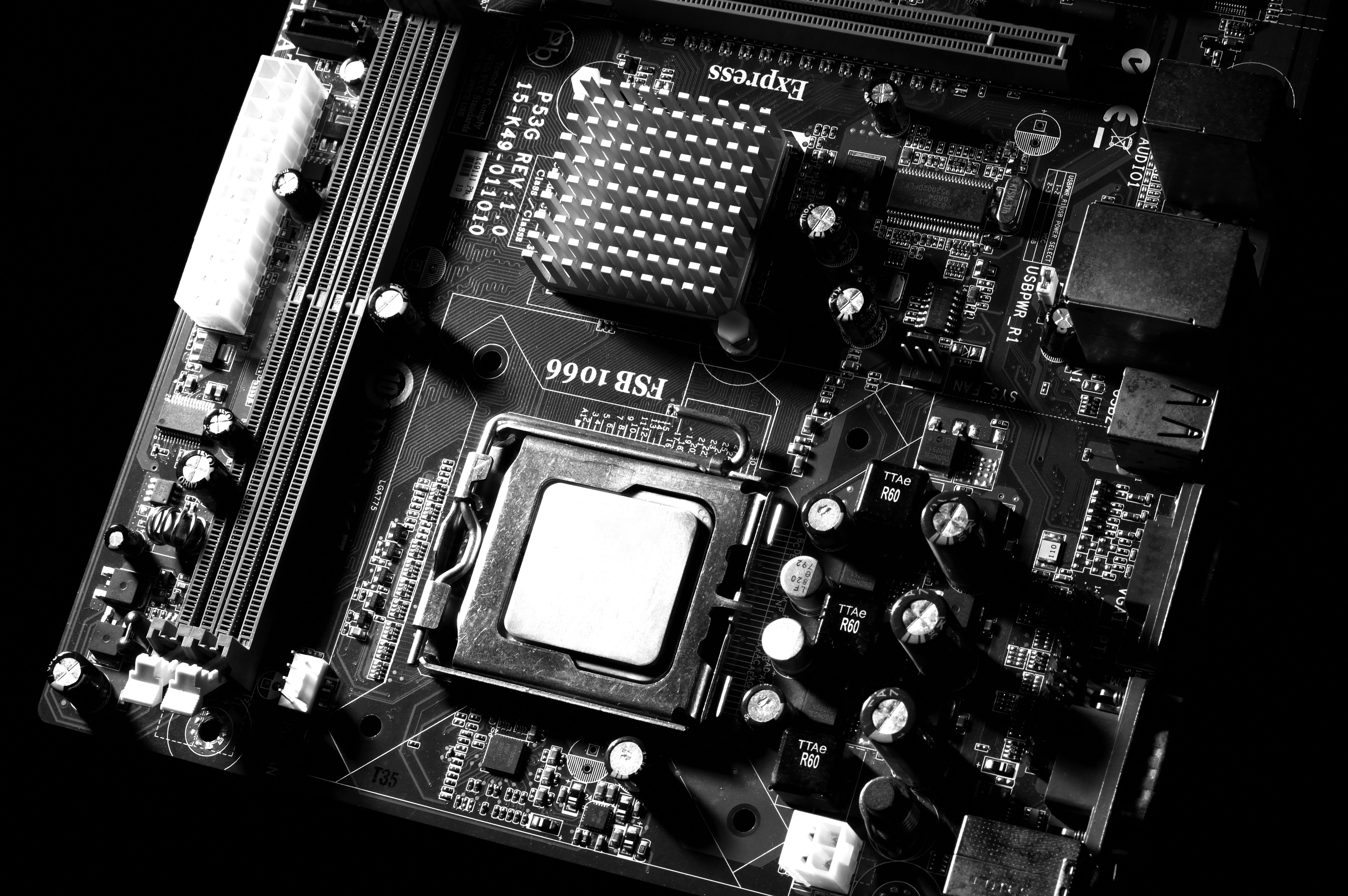
Advantages of low-temperature sintering copper
The core value of low-temperature sintering copper powder is not simply making copper particles smaller, but rather using particle-size control, powder design, and surface treatment to enable strong Cu–Cu bonding and the formation of highly conductive structures at lower processing temperatures.
Currently, copper powder materials in this category can cover particle sizes ranging from approximately 0.15 to 1.30 μm, with material properties tailored to meet the requirements of different applications. Through specialized surface treatments, the oxidation resistance of copper powder can be enhanced while maintaining good sintering performance. In addition, the materials can be formulated with different hydrophilic or hydrophobic solvent systems, providing greater flexibility in formulation and process design.
For printed electronics applications, low-temperature sintering copper powders can be used to formulate copper inks, with certain materials capable of sintering at temperatures of approximately 200°C. This provides a new material option for electronic substrates where process temperature needs to be carefully controlled.
More importantly, low-temperature sintering copper materials are not limited to conventional conductive circuits. Their performance is increasingly being extended to fields such as high-frequency electronics, power semiconductor packaging, and advanced printed electronics.
Potential Applications of Low-Temperature Sintered Copper Powder
1. Power Semiconductor Die Attach and Electronic Packaging
High-current and high-power operation places demanding requirements on power semiconductors, where thermal dissipation and bonding reliability are as critical as electrical conductivity. Low-temperature sintering copper powder can be incorporated into Die Attach Paste (DAP) for bonding semiconductor dies to heat spreaders or heat sinks.
Applications including electric vehicles, power modules, AI power systems, and high-power semiconductors are expected to drive further demand for advanced die attach materials. By reducing material costs while maintaining a balance of electrical conductivity, thermal conductivity, and bonding strength, low-temperature sintering copper powder presents promising potential for next-generation power electronics.
2. Printed Electronics and Conductive Inks
Another promising application is the development of conductive inks based on low-temperature sintering copper powder.
Unlike conventional metal foil or etching processes, printed electronics can form conductive circuits through direct printing of functional materials, potentially reducing certain process steps while providing greater flexibility in circuit patterning.
Copper ink technologies are currently being developed for various printing methods, including screen printing, offset printing, and dispensing.
In addition, emerging technologies such as conformal printing and printing across uneven surfaces or stepped structures are being explored. These developments suggest that future applications of copper inks may extend beyond flat substrates toward more complex three-dimensional structures and localized height differences.
3. High-Frequency Electronics and High-Speed Transmission
As 5G, millimeter-wave communications, AI servers, and high-speed computing continue to advance, the performance of conductive materials under high-frequency conditions is receiving increasing attention.
Beyond good DC electrical conductivity, sintered copper materials also demonstrate promising characteristics for high-frequency applications. This broadens the potential value of low-temperature sintering copper powder beyond simply serving as a low-cost alternative to silver paste, creating opportunities in high-frequency circuits, antennas, RF components, and electronic materials for high-speed signal transmission.
4. Advanced Packaging and Fine-Pitch Interconnects
Beyond die attach and printed electronics, submicron copper powders can also be developed for applications such as die attach pastes for bonding chips to heat spreaders, ceramic substrate interconnects, and fine-pitch circuitry in advanced packaging.
These developments indicate that low-temperature sintering copper powder is evolving beyond its traditional role as a conductive material, toward high-density interconnects, advanced packaging materials, and miniaturized manufacturing processes. This makes it a technology worth closely monitoring for electronic material development where electrical conductivity, processing temperature, and material cost must be carefully balanced.
5. TGV (Through-Glass Via) and Glass Substrates
As high-frequency and high-speed computing, advanced packaging, and heterogeneous integration continue to evolve, glass substrates are attracting increasing attention. Compared with conventional organic substrates, glass offers low signal loss, high dimensional stability, and favorable high-frequency characteristics, making it a promising candidate for next-generation packaging substrates and high-density interconnects.
Among these technologies, TGV (Through-Glass Via) plays an important role in enabling vertical electrical interconnection through glass substrates. A typical TGV process first forms micron-scale vias in the glass, followed by the formation of conductive structures along the via walls through processes such as seed-layer deposition, metal deposition, and electroplating. Achieving a uniform and reliable metal layer within high-aspect-ratio microvias therefore remains a key challenge in TGV manufacturing.
Low-temperature sintering copper powder offers an alternative approach to the development of interconnect materials for glass substrates. Through the optimization of submicron copper powder particle size, surface treatment, and sintering characteristics, its potential use in TGV via filling, conductive structures on glass substrates, and localized interconnects could be further explored.
Compared with conventional metal-processing technologies that require relatively high temperatures, low-temperature sintering copper materials may help reduce the thermal impact on glass substrates and surrounding materials, provided that electrical conductivity, via-filling capability, and substrate reliability can be maintained during sintering.
As glass substrates continue to gain traction in AI, high-performance computing, and advanced packaging, the potential application of low-temperature sintering copper powder in TGV and glass-substrate interconnects represents an emerging area worthy of continued evaluation by material suppliers and semiconductor packaging manufacturers.
Technical Challenges and Future Outlook
Despite its significant application potential, low-temperature sintering copper powder still faces several challenges in practical applications, including oxidation resistance, achieving high sintering density, and compatibility with different substrates. As powder preparation, surface treatment, and sintering technologies continue to advance, these challenges are expected to be gradually addressed. In the future, low-temperature sintering copper powder may find broader applications across the electronics industry and could become an increasingly viable alternative to silver paste.
Overall, as a potential alternative to silver paste, low-temperature sintering copper powder offers the advantages of lower material cost and excellent electrical and thermal performance. With continued technological development and process optimization, its application scope is expected to expand further, creating new opportunities for the electronics industry.
#ConductivePaste #MLCC #SolarEnergy #CopperPowder
#LowTemperatureSintering #AdvancedPackaging #TGV #GlassSubstrate #PowerSemiconductorPackaging
CONTACT US
Kelly Chemical Corporation
Electronics
TEL:(02)2762-1985 ext 11200
Online Message
Leave your contact information,
and we will get in touch with you soon.
Email Consultation
After receiving your email,
we will process it as soon as possible.send Email


