Applications of ultrathin copper foil in high-end electronic and semiconductor packaging
Applications of Ultra-Thin Copper Foil in Advanced Electronics and Semiconductor Packaging
As electronic products continue to evolve toward extreme miniaturization, higher performance, and greater integration, 2–5 μm ultra-thin copper foils and composite copper foils have become key enabling materials for next-generation electronic components and advanced packaging technologies.
1. Characteristics, Specifications, and Development Challenges of Ultra-Thin Copper Foil:
For R&D engineers, reducing copper foil thickness to the 2–5 μm range is far more complex than simply making the material thinner. It requires achieving a new balance among material properties, manufacturing yield, and long-term reliability.
- Development Challenges: Conventional rolled or electrolytic copper foils experience a significant decline in mechanical strength when thickness falls below 5 μm. During high-volume Roll-to-Roll (R2R) manufacturing, issues such as foil breakage, wrinkling, and pinhole formation become increasingly common. In addition, thermal stress and dimensional stability during high-temperature processing present major challenges in the development of high-precision circuitry and semiconductor substrates.
- Required Physical Properties: Beyond extremely low areal density, key performance requirements include high tensile strength, excellent adhesion, low surface roughness, and uniform square resistance. These characteristics are essential for ultra-thin packaging structures and high-density circuit applications.
2. Key Application Areas
Ultra-thin composite copper foil materials are primarily targeted at high-end applications where space, thermal management, and weight are critical considerations.
(1) Advanced Semiconductor Packaging and Substrates: Suitable for High-Density Interconnect (HDI) boards, IC substrates, and fine-line circuit fabrication. The ultra-thin conductive layer helps shorten etching time and significantly reduces undercut effects, while meeting the low-loss requirements of high-frequency signal transmission.
(2) High-Energy-Density Solid-State and Power Batteries: Used as an anode current collector in next-generation solid-state batteries and high-energy-density lithium-ion batteries, substantially reducing copper consumption while improving overall energy density.
(3) Premium Consumer Electronics and Flexible Printed Circuits (FPC): Designed to meet the demanding requirements of foldable smartphones, wearable devices, and other advanced electronics that require maximum space utilization and exceptional flexural reliability.
3. Ultra-Thin Copper Foil and Composite Copper Foil Technologies
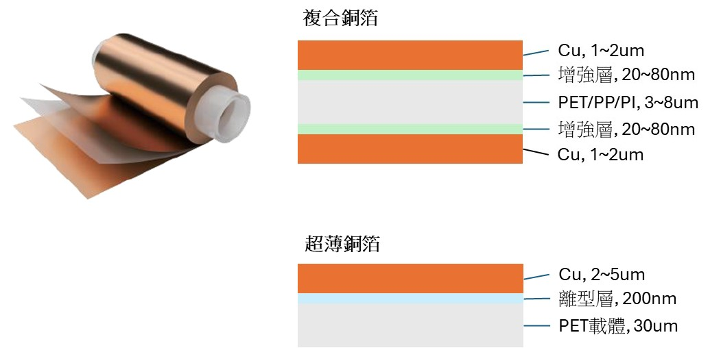
To address these requirements, manufacturers employ a hybrid process combining magnetron sputtering and aqueous electroplating. This technology deposits an ultra-thin, highly uniform copper layer onto polymer substrates such as PET, creating carrier-supported copper foil (Carrier Copper). Alternatively, ultra-thin copper layers can be deposited on both sides of polymer substrates such as PET or BOPET, producing a lightweight and highly functional composite structure.
This advanced copper foil architecture offers several advantages for next-generation product development:
- Extreme Weight Reduction and Space Optimization: Compared with conventional copper foil, composite copper foil leverages the low density of polymer substrates to reduce areal density by more than 50% while maintaining electrical performance. This enables substantial system-level weight reduction and can improve gravimetric energy density by approximately 3–5% within the same volume.
- Superior Mechanical and Interfacial Properties: The material exhibits outstanding toughness and mechanical durability. Both machine direction (MD) and transverse direction (TD) tensile strengths remain at high levels, while excellent elongation at break supports high R2R manufacturing yields. Strong adhesion between the metallic layer and substrate helps prevent cracking and delamination during coating, slitting, and assembly processes.
- High-Precision Process Control: Through advanced process control and precision equipment, double-sided plating thickness can be tightly regulated. Multiple-point measurements ensure that both areal density and sheet resistance remain within ±5% variation. This high level of uniformity supports consistent fine-line etching performance and stable electrical transmission across large-area applications.
- Long Roll Lengths for High-Volume Manufacturing: Long, splice-free rolls reduce roll-change frequency during production, improving equipment utilization and enhancing process continuity in mass manufacturing environments.
The ultra-thin composite copper foil has successfully passed stringent safety evaluations, including puncture testing, while helping reduce battery material costs and overcome the physical limitations of conventional copper foil structures. For R&D teams developing next-generation highly integrated electronic devices, advanced semiconductor packaging solutions, and high-performance energy storage systems, this material offers an optimal balance between manufacturability and end-product performance.
#CopperCladLaminate(CCL) #FlexiblePrintedCircuit (FPC) #ICSubstrate #AnodeMaterials #Lithium-IonBattery (LiB) #HDI #ResinCoatedCopper(RCC) #CorelessSubstrate #CompositeCopperFoil #CarrierCopperFoil
CONTACT US
Kelly Chemical Corporation
Electronics
TEL:(02)2762-1985 ext 11200
Online Message
Leave your contact information,
and we will get in touch with you soon.
Email Consultation
After receiving your email,
we will process it as soon as possible.send Email


